
Page 17 - Shimadzu SPM-9700HT
P. 17
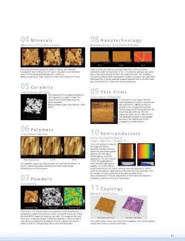
04 Minerals                                   08 Nanotechnology
               Observation of Calcite in Solution            Rendering Images Using Electric Potential


                                                                  Fig. 1        Fig. 2        Fig. 3
               The crystal dissolution process of calcite in solution was observed.   Vector scanning was used on a gold vapor deposition surface on a silicon
               Propagation steps of about 0.3 nm, due to dissolution, were observed.   substrate to render the trace shown in Fig. 1. A conductive cantilever was used to
               About 10 minutes elapsed between (b-1) and (b-3).  apply a tiny electric potential between the sample and probe. After rendering,
               (Data provided by Dr. Kagi, School of Science, The University of Tokyo)  simultaneous AFM and KFM measurements showed no change in the shape of the
                                                             AFM image (Fig. 2), but the potential measured along the trace in the KFM image
                                                             (Fig. 3) was about 50 mV lower than the surrounding area.
               05 Ceramics
               Film Dispersed with Silica                    09 Thin Films
                                 Film material with mono-dispersed spherical
                                 silica dispersed in an organic binder. This   Cross-Section of Thin Film
                                 clearly shows how the binder binds the        A cross-section of an organic thin  lm
                                 spherical particles.                          vapor-deposited on a silicon substrate was
                                 (Data provided by Japan Fine Ceramics Center   observed with the SPM by turning the
                                 (JFCC))                                       sample so the cut edge faced upward.
                                                                               The boundary can be clearly observed. This
                                                                               shows that about the top 1/3 is the
                                                                               organic  lm layer, which is 390 nm thick.
                                                                               This application example is only possible
                                                                               because of the stable probe control
                                                                               provided by the SPM-9700HT.
               06 Polymers
               Li-Ion Battery Separator                      10 Semiconductors
                                                            Electric Potential Analysis of
                                                            Organic Thin Film Transistor (FET)
                                                             This is an example of analyzing
                                                             the shape and electric
                                                             potential of organic thin  lm
                                                             transistors, which have gained
                                                             attention for their use in
                                                              exible displays and other
                                                             applications. The  lm material
                 Room Temperature  125 °C       140 °C
                                                             is P3HT (3-hexylthiophene),
               The separator surface was observed after removal from the lithium-ion   which provides high electron
               battery. Heated observation shows how the  ber swells at high   mobility. To use the SPM for
               temperatures and  lls the pores.              actual measurement, the source electrode was grounded and an electric
                                                             potential was applied independently to the gate and drain electrodes, then
                                                             the variation in surface potential on the gate was determined.
                                                             (Data provided by Dr. Fukuda, Department of Information and Electronic
               07 Powders                                    Engineering, Muroran Institute of Technology)
               Toner Particle
                                                             11 Coatings
                                                             Baking Finished Surface


                 Topography image  Phase image  Potential image
               The top part of one toner particle was observed at high magni cation. A
               topographic image of the surface is shown on the left. Phase and surface
               potential (KFM) images are shown on the right. The images on the right
               show how comparing images of different properties in the same  eld of
               view allows correlating the distribution of toner material and external   The coated surface shows many holes from outgassing. The metallic painted
               additives with the corresponding electric potential distribution.   surface (left) shows it contains metal  bers.


                                                                                                                  17