
Page 6 - Electric&Electronics - Total Solution for Analyzing Electronic Devices
P. 6
Observation and Analysis/Evaluation
Micro-Area Observation
● 3D Measurement and Physical Property Measurement of Nano-regions High Resolution Scanning Probe Microscope/Atomic Force Microscope
● Observation of Micro-Shapes on Sample Surfaces, LCD Panel Alignment Films, or ITO Membranes SPM-8100FM
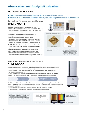
Scanning Probe Microscope/Atomic Force Microscope
SPM-9700HT
The HR-SPM represents a new generation of scanning probe microscopes
A scanning probe microscope (SPM) is a generic term for based on frequency detection. Previous scanning probe microscopes
microscopes that scan sample surfaces with a tiny probe to observe (SPM)/atomic force microscopes (AFM) were generally based on amplitude
three-dimensional shapes at high magni cations. A common type of modulation (AM). However, in principle, frequency modulation (FM) offers
SPM is an atomic force microscope (AFM). higher sensitivity for acquiring higher-resolution images.
LSI Circuit Observation Example Quantum Dots In addition to ultra-high-resolution observation either in air or liquid, it also
・Samples can be observed at high magni cations in an
atmospheric environment. enables, for the rst time, observation of hydration/solvation at the
・Even insulative samples can be observed directly. solid-liquid interface.
・Samples can be accurately measured in their height direction. HR-SPM Features
・Physical quantities other than height, such as surface potential, ・Uses FM-based scanning.
magnetic force, viscosity, and elasticity, can also be measured. ・Noise levels in air and liquid are reduced to 1/20 of the previous model.
・Performance levels of vacuum SPM models are achieved in air and liquid.
The SPM-9700HT enables observation of metals, semiconductors,
ceramics, organic substances, polymers, and biological samples at ・Enables measurement of local structures at the solid-liquid interface.
high resolutions in an atmospheric environment without coating or The circuit patterns and contact holes in This shows the observation of In0.7Da0.3As ・Equipped with an HT scanner for a larger observation area and even faster speeds.
other pretreatment. It can obtain images of sample surface large-scale integrated (LSI) circuits can be quantum dots grown by molecular beam epitaxy ・Dual monitors and signal display function dramatically improve exibility.
observed clearly. (MBE) on a GaAs (100) substrate (2-degree tilt).
unevenness at high magni cation rates ranging from a few AFM images can provide information important
thousand times to several million times. It also offers superior for opto-electronics, such as the density, shape,
and regularity of quantum dots. (Source: MJ. da
resolution with respect to the vertical direction of the sample, which
Silva, Prof. A.A. Quivy, University of São Paulo) Differences from Previous SPM/AFM Systems
enables accurate measurement of material surface roughness.
Observation of Atomic Resolution
in Liquid
Scanning Probe Microscope/Atomic Force Microscope
SPM-Nanoa
The SPM-Nanoa achieves high-resolution observation by adopting a high-sensitivity low-noise detection
optical mechanism, and also automates the optics adjustment and observation parameter setting steps, a
manual process with previous models. Consequently, even inexperienced users can easily obtain
high-resolution observation data.
It can be used for a wide variety of nanotechnology or nanoscience issues by observing the shape or
evaluating the physical properties of polymer materials, battery materials, nanomaterials, and so on.
2.0 × 2.0 nm
AM Method FM Method
Automatic light Automatic observation Image processing
Cantilever setting beam adjustment Sample placement
AUTO AUTO AUTO
KPFM* Observation of Pt Catalyst
Particles in Air
The SPM-Nanoa helps achieve stress-free observations by automating steps that required practice with
previous SPM models, such as adjusting the light beam, adjusting parameter settings during observations, and *KPFM: Kelvin Probe
processing image data. Force Microscope -0.80 0.25
[V]
[V]
Operating time when using standard samples and standard cantilever: About 5 minutes*
* For automatic observation with a 1 m eld of view and 256 × 256-pixel resolution. Actual operating times can vary depending on the operator.
This is an example of analyzing the shape and electric potential of S G D S G D Source: Prof. Fukuda, Department of
organic thin lm transistors, which have attracted attention for use in Electrical and Electronic Engineering,
exible displays and other applications. The lm material is P3HT P3HT Faculty of Engineering, 50.00 nm 100.00 × 100.00 nm 50.00 nm 100.00 × 100.00 nm
Source Drain
(3-hexylthiophene), which provides high electron mobility. Insulator Muroran Institute of Technology
To use the SPM for actual measurement, the source electrode is Gate AM Method FM Method
grounded and electric potentials are applied independently to the gate
and drain electrodes, as diagrammed to the right, to map the variation V G V D
in surface potential at the top of the gate.
Measurement Schematic Diagram VG=-10V,VD=-40V
Height Potential
6 7