
Page 5 - Electric&Electronics - Total Solution for Analyzing Electronic Devices
P. 5
Comprehensive Quantitation Functions
Observation and Analysis/Evaluation
Micro-Area Observation and Elemental Analysis Elemental Analysis and Chemical State Analysis
● Submicron Contaminant Analysis and Elemental Analysis of Intermetallic Compounds, ● Composition/Bond State Analysis of a Sample's Surface and Metal Surface Discoloration Analysis
Such as Solder Joints for Mounted Devices
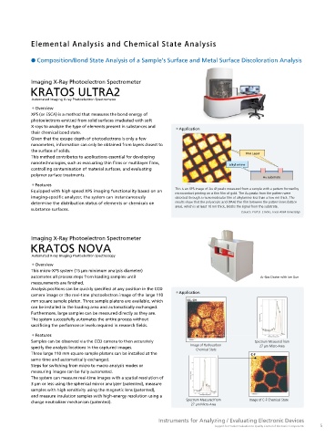
Electron Probe Microanalyzer Imaging X-Ray Photoelectron Spectrometer
EPMA-1720 Series KRATOS ULTRA2
Automated Imaging X-ray Photoelectron Spectrometer
Using only simple mouse operations, EPMA-1720 series ・Overview
microanalyzers can reveal the micron, submicron, and even XPS (or ESCA) is a method that measures the bond energy of
nano-level microstructures in electrical/electronic materials.
photoelectrons emitted from solid surfaces irradiated with soft
・Enables analysis of submicron-level contaminants or the identity, X-rays to analyze the type of elements present in substances and ・Application
shape, and quantity of impurities. their chemical bond state.
・Non-uniformities and segregations can be determined from Given that the escape depth of photoelectrons is only a few
element distributions over a large 90 × 90 mm area. nanometers, information can only be obtained from layers closest to
・Multiple samples can be analyzed successively without human the surface of solids. PAA Layer
intervention. This method contributes to applications essential for developing
nanotechnologies, such as evaluating thin lms or multilayer lms, alkyl amine
Cu Migration between Printed Circuit Boards Analysis of LED Eutectic Mount Plating Layer controlling contamination of material surfaces, and evaluating
polymer surface treatments.
Optical Microscope Image Cu Au substrate
・Features
This is an XPS image of Au 4f peaks measured from a sample with a pattern formed by
Equipped with high-speed XPS imaging functionality based on an
microcontact printing on a thin lm of gold. The Au peaks from the pattern were
imaging-speci c analyzer, the system can instantaneously detected through a monomolecular lm of alkylamine less than a few nm thick. The
determine the distribution status of elements or chemicals on results show that the polyacrylic acid (PAA) thin lm between the pattern lines (lattice
area), which is at least 10 nm thick, blocks the signal from the substrate.
substance surfaces.
(Source: Prof D. Crooks, Texas A&M University)
Cl
1mm 2 m 2 m 2 m 2 m
BSE Ag Sn Mo
Migration direction
Resist lm
Cu pattern
An EPMA-1720H model equipped with a high-resolution CeB6 electron gun clearly Imaging X-Ray Photoelectron Spectrometer
Board
(+) (-) shows the ne structure of the LED eutectic mount plating layer. It shows that the Sn in
the plating layer applied to the Ag layer is bleeding into the Ag layer. KRATOS NOVA
This is an example of analyzing a contaminant on a
circuit board. It shows that the Cu is migrating from the The thin lm of Mo is about 0.4 µm thick. Automated X-ray Imaging Photoelectron Spectroscopy
cathode (-) toward the anode (+). A distribution of Cl is
also present at roughly the same location as the Cu.
・Overview
This micro-XPS system (15 µm minimum analysis diameter)
automates all process steps from loading samples until Ar Gas Cluster with Ion Gun
measurements are nished.
EPMA-8050G Analysis positions can be quickly speci ed at any position in the CCD ・Application
camera image or the real-time photoelectron image of the large 110
mm square sample platen. Three sample platens are available, which
The EPMA-8050G features a high-intensity Schottky emitter and a can be installed in the loading area and automatically exchanged.
new electron optical system that can focus the electron beam to a Furthermore, large samples can be measured directly as they are.
smaller diameter, which achieve high spatial resolution even during The system successfully automates the entire process without
irradiation at high current levels. sacri cing the performance levels required in research elds.
・Achieves the world’s highest spatial resolution performance during ・Features
high-current irradiation. Samples can be observed via the CCD camera to then accurately Spectrum Measured from
・Enables ultra-high-sensitivity analysis with irradiation at high specify the analysis locations in the captured images. Image of Hydrocarbon 27 µm Micro-Area
current levels up to 3 µA. Three large 110 mm square sample platens can be installed at the Chemical State
・With a large 52.5-degree X-ray take-off angle, it can even analyze same time and automatically exchanged.
bumpy samples with excellent accuracy. Steps for switching from micro to macro analysis modes or
measuring images can be fully automated.
COMPO 1 µm Ag 1 µm Cu 1 µm
The system can measure real-time images with a spatial resolution of
This data is from mapping analysis of an area of a lead-free solder that contains a high
concentration of Ag. (Accelerating voltage: 10 kV, Irradiation current: 20 nA) 3 µm or less using the spherical mirror analyzer (patented), measure
The particle shape in the X-ray image of Ag closely matches the particle shape in the samples with high sensitivity using the magnetic lens (patented),
BSE image (COMPO). It shows that the particles circled with a red dashed line, which
appear to have a 0.1 µm diameter, are also Ag particles. It also shows the presence of and measure insulation samples with high-energy resolution using a Spectrum Measured from Image of C-F Chemical State
particles that contain Cu, which are indicated circled with a yellow dashed line. charge neutralizer mechanism (patented).
27 µm Micro-Area
4 5