
Page 6 - Shimadzu Axis Supra+
P. 6
HIGH THROUGHPUT SAMPLE HANDLING –
A B
TYPICAL WORK FLOW
To guarantee high sample throughput, up to 3 sample holders may be
placed on the Flexi-lock sample magazine. An optical image is acquired
of each sample holder from which the sample analysis positions are
identified during the automated ‘pump’ cycle. An acquisition method is 75mm
chosen defining all requirements for the data acquisition. A method may
define simple spectroscopy or more complex experiments such as sputter
depth profiling or angle-resolved XPS. Subsequent analysis from samples 32mm
on different sample holders can be added to the analysis queue with the
automated sample handling system exchanging the sample holder to C D
progress through the analysis queue.
+
Key attributes of AXIS Supra automated sample handling:
• Automated, unattended sample holder exchange.
• High throughput, rapid sample analysis.
• Ideal for a multi-User environment.
2
2
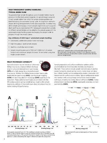
• Sample mounting area up to 7200 mm (2400 mm x3 sample AXIS Supra sample holders: (A) Dual height sample holder.
+
holders) with maximum sample thickness 19 mm (when using dual (B) Combination sample holder, including 15mm diameter stub for
height sample holder). use with accessories. (C) Azimuthal rotation sample holder. (D) Heat
and cool sample holder.
MULTI-TECHNIQUE CAPABILITY
Optional excitation sources include an achromatic Sample preparation and surface modification options can be
Al/Mg X-ray source, improved Helium discharge accommodated on the introduction chamber, also known as
lamp for ultraviolet photoemission spectroscopy Flexi-lock. These options include sample heat and cool, air sensitive
(UPS) and a high energy Ag La monochromated sample transporter, broad spot ion source, crystal clever and glove
X-ray source. Addition of a field-emission electron source adds box. A third chamber can be configured to provide a dedicated UHV
Auger electron spectroscopy (AES), scanning Auger mapping environment for surface science studies. Typical configuration equips
(SAM) and secondary electron microscopy (SEM) capability to the this chamber with a manual stage and optional characterisation
instrument. These additional techniques are coincident with the techniques including low energy electron diffraction (LEED), inverse
XPS analysis position giving complementary insight to the sample. photoemission spectroscopy (IPES), quadrupole secondary ion mass
Importantly addition of these techniques does not compromise the spectrometry (SIMS).
market leading XPS performance.
PET PMMA Nylon6 PEEK
Si
A B elem
2.5nm Si N Si N 4
Si N
Counts per second SiO 2 Si Substrate Counts per second SiO 2 Normalised (arb. units)
2nm HfO
3
3
4
1nm SiO
Si
elem
107 105 103 101 99 97 95 93 108 105 102 99 96 93 20 15 10 5 0
Binding Energy / eV Binding Energy / eV Binding energy (eV)
Si 2p spectra acquired from thin film multilayer sample (courtesy of IMEC) He II excited UPS valence band spectra of four common
shown in the schematic figure using (A) monochromated Al Ka radiation and (B) polymers.
monochromated Ag La. The greater information depth of the Ag La excited Si 2p
spectrum is demonstrated by the larger Si elemental substrate component.
6