
Page 20 - Material Characterizations
P. 20
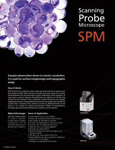
Scanning


                                                                                    Probe


                                                                                    Microscope


                                                                                   SPM


          Sample observation down to atomic resolution.
          It is used for surface morphologic and topographic

          study.


          How It Works
          SPM consists of a cantilever with a sharp tip at its end that is used to scan
          the sample surface. When the tip is brought into close range of a surface,
          forces between the tip and surface cause a deflection of the cantilever. A
          laser spot is used to measure the deflection by reflecting it off the top
          surface of the cantilever onto a detector. Several forces can be imaged,
          measured and even manipulated. Some common examples are mechanical
          contact force, magnetic force, electric current etc. Measurements can be
          done in air, vacuum or liquid environment. Effects of temperature,
          humidity, gas and electrochemistry on samples can be studied.

          Major Advantages     Areas of Application                                   SPM-8000FM

          Ultra high resolution analysis   • Living organisms, eg. E.coli bacteria
          of surface of materials.   • Metals, eg. boundary surface of plating layer
          A wide variety of sample   • Non metals, eg. ferroelectric domains
          characteristics can be   • Minerals, eg. observation of calcite in solution
          analysed. Relevant to a   • Ceramics, eg. film dispersed with silica
          big spectrum of industry.  • Polymers, eg. Li-ion battery separator
                               • Powders, eg. toner particle
                               • Nanotechnology, eg. rendering images using
                                  electric potential
                               • Thin films, eg. cross-section of the film
                               • Semiconductors, eg. electric potential analysis of
                                  organic thin film transistor
                               • Coatings, eg. baking finished surface                SPM-9700


    24  Excellence in Science